
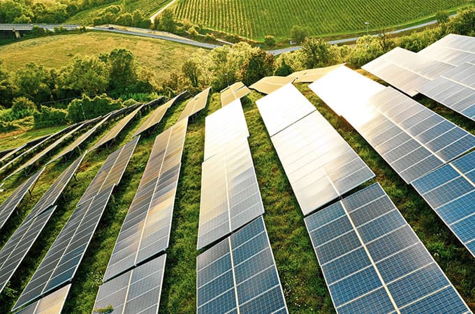
Improving energy efficiency is a constant pursuit of manufacturing engineers’ process innovations, including reducing materials and labor used in the manufacturing process, and maximizing the effective use of components and the amount of electricity generated per unit area. The precision of laser processing allows photovoltaics to improve energy efficiency from the manufacturing side. Specifically, as in the vapor deposition process for battery fabrication, laser processing provides higher yields at a lower cost than other deposition methods, reducing the additional materials required for chemical deposition.
In addition, we can also see other applications of laser technology in solar cell manufacturing, including:
Battery edge passivation: A key factor in improving solar cell efficiency is minimizing energy loss through electrical isolation, typically accomplished through silicon wafer edge etch passivation. Traditional processes use plasma to treat edge insulation, but the etching chemicals used are expensive and environmentally harmful. Using a laser with high energy and high power can quickly passivate the cell edges and prevent excessive power loss. With laser-shaped grooves, the energy loss due to solar cell leakage current is greatly reduced, from the 10-15% loss of traditional chemical etching processes to the 2-3% loss of laser technology.
Line up: In addition to improving energy efficiency, laser technology also makes many process tasks easier in the manufacturing process. Aligning silicon wafers with a laser is a common online process for the automatic stringing of solar cells. Connecting solar cells in this way reduces storage costs and allows for neater, more compact strings of cells per module.
Dicing: The laser can be used as a cutting tool in the silicon wafer and cell processing. Cutting silicon wafers by laser is the most advanced at present. It has high precision, high repeatability, stable work, fast speed, simple operation, and convenient maintenance.
Wafer marking: A notable application of lasers in the silicon photovoltaic industry is the marking of silicon wafers without affecting their conductivity. Wafer marking helps manufacturers track their solar supply chain and ensure consistent quality.
Thin-film ablation: Thin-film solar cells rely on vapor deposition and dicing techniques to selectively ablate certain layers to achieve electrical isolation. The layers of the film need to be deposited quickly without affecting other layers of the substrate glass and silicon. Instantaneous ablation can cause circuit damage on the glass and silicon layers, leading to battery failure.